Hardware and Wiring
What the AEH-W41H1 module is, what is on its board, and the 4-pin port it plugs into. Read this before you build a replacement board or put a clip on the module.
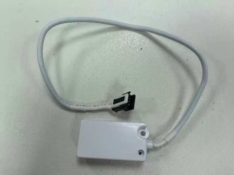
The module: a small board in a white housing on a 4-pin cable to the indoor unit. (Photo: FCC ID 2AGCCAEH-W41H1, public record.)
The module is a sealed plastic dongle. Its connector carries 5 V, GND and an RS-485 A/B pair. Under an RF shield sit the Wi-Fi chip and its flash. The RS-485 transceiver is outside the shield, next to the cable connector.
More detail: reverse-engineering/docs/01-hardware.md and reverse-engineering/hardware/pinouts.md.
What is on the board
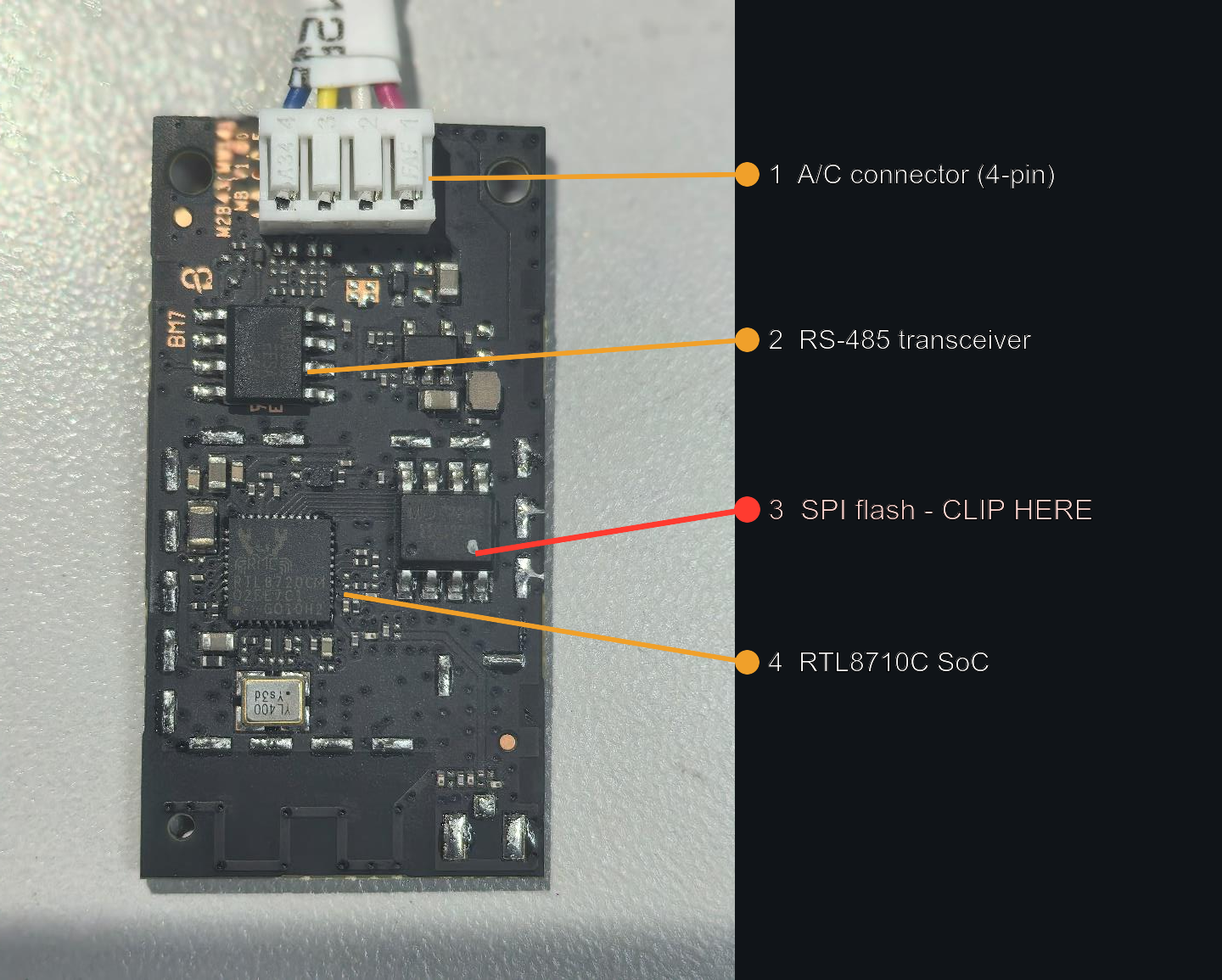
RF shield removed. 1: the 4-pin A/C connector. 2: the RS-485 transceiver. 3: the SPI flash (the clip goes here). 4: the RTL8710C. Photo: FCC ID 2AGCCAEH-W41H1, public record.
| Part | Detail |
|---|---|
| Wi-Fi chip | Realtek RTL8710C (AmebaZ2 family), ARM Cortex-M, Wi-Fi and BLE. Secure boot is off. ESPHome runs on it through the LibreTiny platform (The Stock Module) |
| Flash | GigaDevice GD25Q32(B): 4 MB SPI NOR, SOIC-8, JEDEC ID C8 40 16. Two firmware slots, and a settings area near the top |
| RS-485 transceiver | Union Semiconductor UM3352E, MAX485-compatible, SOIC-8 |
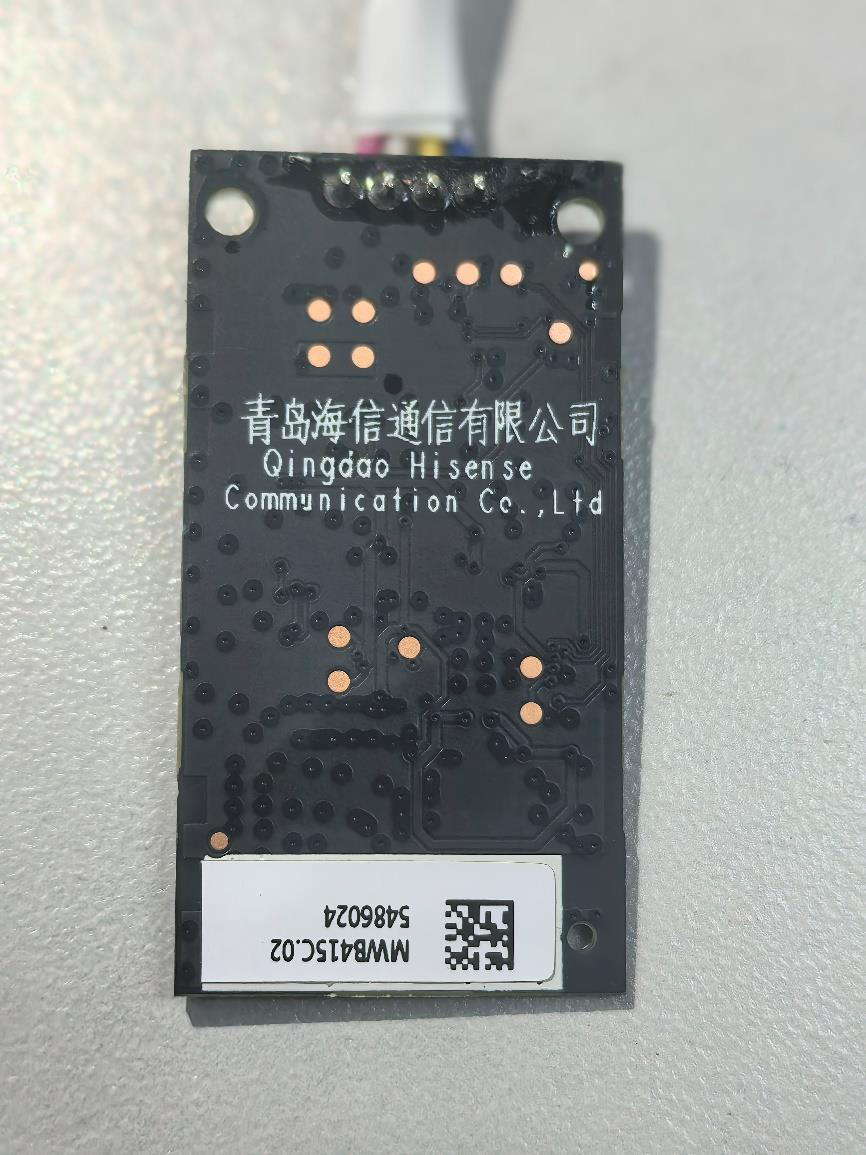
The underside of the board carries the model marking (FCC ID 2AGCCAEH-W41H1, public record).
The 4-pin A/C port
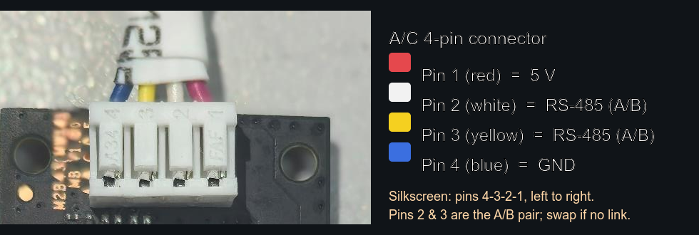
The board silkscreens the pins 4-3-2-1 from left to right.
| Pin | Signal | Wire colour on the bench unit |
|---|---|---|
| 1 | 5 V | red |
| 2 | RS-485 A or B | white |
| 3 | RS-485 A or B | yellow |
| 4 | GND | blue |
A and B are interchangeable at wiring time. If the bus does not link, swap them. Wire colours can differ between revisions, so check them on your own unit before you power anything.
Power comes from the A/C. A bench supply tends to brown out the radio, so run the module, or the board that replaces it, from the unit.
The bus
- RS-485, half duplex, 9600 baud, 8N1. The module is the bus master and the A/C mainboard only answers (Protocol Overview).
- On the module the bus is UART0: TX on
PA_14, RX onPA_13, and the transceiver’s driver enable (DE) onPA_17. The firmware raises DE around every transmission, as the vendor firmware does. The module’s log console is onPA_16. - On the UM3352E, bus A and B are pins 6 and 7. RO (pin 1) carries the bytes from the A/C at logic level, and DI (pin 4) the bytes to the A/C. Both are good points for a sniffer. The logic level is probably 5 V, so shift it to 3.3 V before a 3.3 V adapter.
Access to the flash
The GD25Q32 can be read and written with a CH341A programmer and a SOIC-8 clip. The wiring, the in-circuit read problem and the CH341A voltage warning are in Recovery and Reflash.
Next
- To replace the module with an ESP32: ESP32 Replacement Board, which has the parts, the pin tables and the wiring picture.
- To keep the module: The Stock Module, and take a full dump with the clip before anything else.